PHY2028 SimSheet-04
SPICE simulations of FET circuits
Homework
Read Storey (1998) ch. 6 / Storey (2006) ch. 7 and/or the Interfet Corporation Aplication Note [pdf]. For the purposes of PHY2028, you do not need to know about the details of how FETs work, just what they do and some examples of how they are used.
- Explain what is meant by the:
- slew rate (SR),
- gain-bandwidth product (GBW),
- common-mode rejection ratio (CMRR),
of an op-amp.
- Design a two-stage direct coupled amplifier with a voltage
gain of 12. Your circuit should use two BC107 bipolar
transistors, operate from a 12V supply, and have a maximum
output swing (peak-peak) of at least 5V. You may wish to
refer to Storey (1998) example 7.7 / Storey (2006) example 8.11.
- Explain, with an illustrative example, what is meant by
the Miller effect
Practical Session
Design and simulate a subtractor circuit with a gain of 100, i.e. Vout = 100(V2 - V1), based on the LM741/NS op-amp model in PHY2028.LIB. Use simulations to determine the SR and GBW for the model. Also plot the CMRR (in dB) as a function of frequency from 10Hz to 1MHz (MegHz not mHz!) and compare your results with the 741 data-sheet you used in the laboratory. [Note: The model in PHY2028.LIB includes some offset errors.]
Milestone 1
Simulate your design (above) for a two-stage bipolar transistor amplifier. Use a tran analysis to demonstrate that your design meets the output swing specification, and an ac analysis to plot its frequency response.
Milestone 2
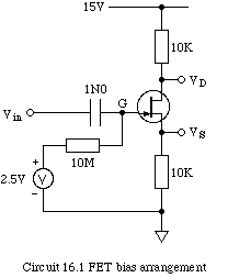
Download CW121004-01.CIR and use it to plot characteristic curves for the 2N4416 JFET device. Draw a diagram of the circuit being used and identify the saturation region and resistive regions on the first plot. Use the second plot to estimate the quiescent values of VS and VD for circuit 16.1 (below). Check your answer by running a simulation. If the input signal is a 1V 1kHz sine-wave, what are the amplitudes at the two outputs? [Note: The n-channel JFET model is explained in §3.4.5 of the User's Guide.]
Milestone 3
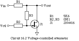
Circuit 16.2 is a voltage-controlled attenuator. Run a Spice tran simulation several times using different values for Vctl and hence plot a graph of gain (in dB) against Vctl. Use a 0.25V amplitude 1kHz sinewave for Vin and keep Vctl<0V. With the gain at -20dB, determine the maximum amplitude of Vin that can be used without serious distortion.
Milestone 4
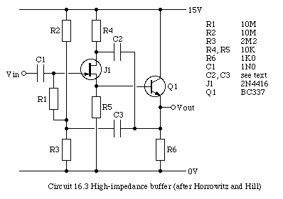
Circuit 16.3 is a high-speed high-impedance buffer from Horowitz and Hill (2nd edition) p. 172 with minor corrections. Simulate this circuit, initially omitting C2 and C3, and use Spice to plot the input impedance as a function of frequency from 10Hz to 10MHz.
Now include C2 and C3 (both 100nF) in the simulation and, once again plot the input impedance.
[Note: This type of bootstrap circuit has a high input-impedance but compromises the noise performance and stability to do so. There is no free lunch here.]
Milestone 5