You can see the abstract if you wish.
To understand our motivations in studying this system, please see our overview of Surfactant Mediated Growth.
It has long been known that the clean Si(001) surface reconstructs into at least a (1x2) structure by the formation of dimers (bonded pairs of atoms) at the exposed surface. What has been an issue of some debate is the question of whether these dimers are symmetric (i.e. both atoms lying at the same distance above the substrate) or asymmetric (i.e. buckled). A possible geometry is shown below. Please note that although the image is of symmetric dimers we are not making such a claim here: the image is for illustrative purposes only. Click on the image to download a larger version. If you have a viewer for .xyz files (e.g. xmol) then you can download the geometry and play with it yourself....
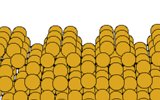 Let us define our co-ordinate system with reference to this system as follows: the direction perpendicular to the surface is the z-direction, the direction along a given dimer is the y-direction, and the direction along a given dimer row is the x-direction. Because the periodicity is doubled along the y-direction, but remains the same along the x-direction, we call such a surface (1x2).
Upon deposition of Sb (Antimony), the Si dimers are broken apart and the surface is instead characterised by Sb dimers which are arranged in rows perpendicular to the Si dimers found on the original clean surface. For this reason we refer to the reconstruction as (2x1), in contrast to the (1x2) reconstruction of the original clean surface (of course, depending on how we view the surface, we could just as easily swap these designations as long as we retain the distinction between the two reconstructions).
We have performed first principles pseudopotential LDA calculations (using the EKSETER code) on the Sb-covered Si(001) surface, determing the structure shown below. A (1x1) structure with no dimers is also possible, but we calculate that it is unstable relative to the (2x1) structure (the energy difference between the two structures is 0.10 eV per dimer). The (1x1) surface is metallic, and it is the saturation of one partially occupied dangling bond per Sb atom which explains the stability of the dimerised surface.
In the image below, the Sb atoms are shown in purple. Note also that we are now viewing the surface along the direction perpendicular to the viewing direction used for the clean surface (above):
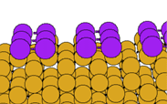 Once again, you can download the geometry in .xyz format, or click on the image to see a larger version.
The Sb dimers are symmetric, in agreement with previous theoretical studies (Cho and Kang, Phys. Rev. B51, 5058 (1995); Tang and Freeman, Phys Rev B47, 1460 (1993)). Our calculated Sb-Sb and Sb-Si bond lengths are also in accord with previous theory, and with experiment (Richter et al, Phys. Rev. Lett. 65, 3417 (1990)).
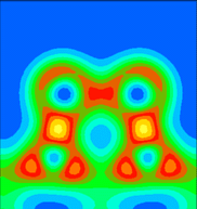
It is instructive to examine the total valence charge density for the system. Click on any of the images below to download a enlarged view, including numerical values for the density.
It is important to note that these images show only the valence electron density, since they were calculated using the pseudopotential method. Thus the atomic core sites show up as minima in the valence electron density (blue), while bonds show up as maxima (red/yellow).
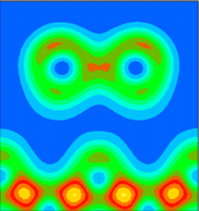 This is a vertical plane chosen to cut through the Sb dimer, i.e. y=0.0 (in lattice co-ordinates). The nearest neighbours of the Sb atoms do not feature in this plot, because they are located on the plane y=0.5.
 This is another vertical plane, chosen to include the nearest neighbours of the Sb dimer, i.e. y=0.5 (in lattice co-ordinates). The Sb dimer itself does not appear since it lies on the y=0.0 plane. Clearly there is some charge transfer to the Si-Si bonds which lie nearest to the Sb dimer, at the expense of those which are further away.
 An angled plane has been chosen here, to include both the Sb dimer atoms and the nearest neighbour Si atoms. That is, it includes the Sb-substrate bonds. Note that these are much stronger than the bonds between the two Sb atoms.
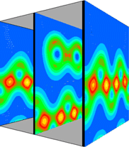 This view combines the y=0.0 and y=0.5 planes to give a 3D impression of the total valence electron density.
Our calculated electronic band structure for the system is shown below. The blue shaded region is the projection of the bands of bulk Si onto the (001) surface Brillouin zone. The additional bands are those which are associated with the surface. There are two fully occupied bands in the band gap and one unoccupied band. The (2x1) structure is semiconducting, unlike the (1x1) structure mentioned earlier.
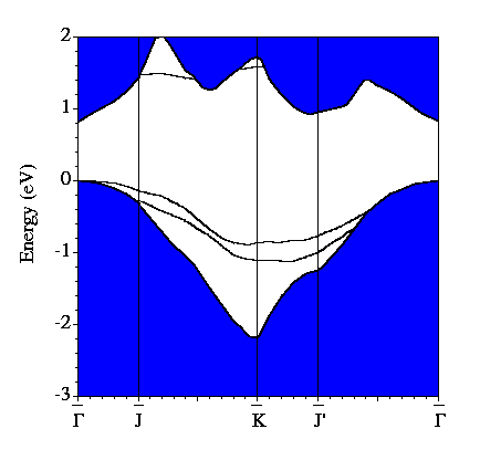
By examining the valence charge density associated with individual states we have determined that the two occupied surface bands are due to pi-ungerade and pi-gerade (bonding/antibonding) combinations of the remaining Sb dangling bonds. The notation "gerade" implies symmetry under inversion with respect to the bond centre, while "ungerade" means the orbital is asymmetric. You can see these two combinations below. Normally for pi orbitals the ungerade orbital lies lower in energy than the gerade orbital. The reversal of this normal ordering for the present situation is very interesting.
 This is a vertical y=0.0 slice through the higher lying of the two bands (at the K-point). It is a pi-ungerade combination of pz-like dangling bonds and might ordinarily be expected to make a significant contribution to the strength of the dimer bond.
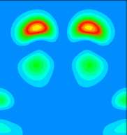 This is a vertical y=0.0 slice through the lower lying of the two bands (at the K-point). It is a pi-gerade combination of pz-like dangling bonds. In, for example, the carbon dimers at the diamond (001) surface, such a band would lie at higher energy than the pi-ungerade bonding orbital. Here, because of the extra two electrons per Sb dimer (as compared to the carbon dimer), the pi-gerade orbital is occupied. This results in additional electron-electron interactions which not only lower the energy of the band below the pi-ungerade orbital, but also change the dispersion of the band so that it follows that of the pi-ungerade orbital very closely.
The contribution of the pi-ungerade bonding orbital to the strength of the dimer bond is largely cancelled by the effect of the pi-gerade antibonding orbital. The main contribution to the dimer bond therefore comes from the sigma bond formed by px-like Sb dangling bonds. This band lies at energies far below the band gap region and thus does not appear in the band structure shown above.
The unoccupied surface state visible in the band structure is located in the first two layers of the Si substrate.
In conclusion, we have studied the geometry of the Si(001)(2x1)-Sb system and find that our results for bond lengths are in agreement with previous theory and with experiment. We also present the first thorough explanation of the nature of the Sb dimer bonding. We find that the main contribution to the dimer bond is from sigma bonding of px orbitals, while fully occupied pi-ungerade and pi-gerade orbitals cancel each other. The role of these orbitals in the adsorption of Ge onto the Sb covered surface will be the focus of future work.
We hope you have enjoyed reading this page. If so, why not e-mail us and let us know ? Preprints/reprints can be requested by e-mail or at the addresses quoted on our home pages.