You can see the abstract if you wish, or download the text of the paper in tex format.
The molecular-beam-epitaxy grown GaAs(001) surface is one of the most studied polar semiconductor surfaces, due to its importance for electronic and photonic devices. A whole range of experimental techniques have recently been employed to investigate the atomic and electronic structure of this surface.
We are interested in growth upon the GaAs(001) substrate as part of our work on Surfactant Mediated Growth. Initially we have studied the clean GaAs surface, but future work will tackle growth on this substrate.
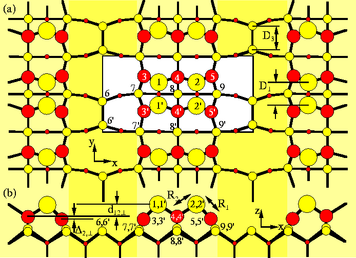
The ideal GaAs(001) surface is terminated with either Ga or As atoms. In experimental growth conditions up to seven different reconstructions of this surface have been reported as a function of stoichiometry (i.e. with different proportions of Ga and As). Previous theoretical and experimental work suggests that the most likely structure for the As-terminated surface unit cell is the one shown below, with As atoms marked in yellow and Ga in red. The main features of this reconstructed surface are the parallel rows of trenches, separated by blocks made up of top-layer As dimers sitting on second-layer Ga atoms.


| D1 (Angs.) | D3 (Angs.) | d12 (Angs.) | Delta2 (Angs.) | R1 (Angs.) | R2 (Angs.) |
|---|---|---|---|---|---|
| 2.39 | 2.50 | 1.26 | 0.30 | 2.28 | 2.42 |
The most notable feature of the geometry we have calculated is the relaxation of the second layer Ga atoms on the edge of the dimer block (marked 3, 3', 5 and 5' above) towards the centre of the dimer block. This is because they are only three-fold co-ordinated (i.e. they form bonds with only three neighbouring atoms). In bulk GaAs the Ga atoms would be bonded to four neighbouring atoms, and the electrostatic repulsion between the electrons in the bonds would force the bond angles to be tetrahedral. Now, with only three bonds the repulsion will force the bonds into an almost trigonal planar geometry (i.e. all the bonds will lie in a plane, with bond angles of 120 degrees). In order to achieve this these Ga atoms must relax in the manner shown in the figures above.
In contrast, the second layer Ga atoms lying along the centre-line of the dimer block (marked 4 and 4' above) are still four-fold co-ordinated, and so move far less from their ideal positions when the structure is allowed to relax.
The different relaxations of the Ga atoms at the edge of and in the centre of the dimer block leads to a bimodal distribution of Ga-As bond lengths. That is, the bond length between, say, atom 2 and atom 5 (R1) is different from that between atom 2 and atom 4 (R2). Also, there is a small vertical separation between different Ga atoms in the second layer (Delta2).
A more detailed analysis of the structural and bonding information we have calculated is presented in the paper to appear in Physical Review B on 15th May, 1996.
A particularly interesting feature of this surface is found to be the bimodal distribution of Ga-As bond lengths between the first and second layers. This is due to the presence of both three- and four-fold co-ordinated Ga atoms in the second layer. Our findings regarding charge density and bond lengths should prove complimentary to existing theoretical and experimental results, notably from LEED, RHEED and STM studies. Furthermore, it is hoped that this work wil stimulate future experimental work, particularly using x-ray standing wave and SEXAFS techniques, to confirm the structural parameters we have calculated, so that we may gain a better understanding of this fascinating and technologically important surface.
We hope you have enjoyed reading this page. If so, why not e-mail us and let us know ? Preprints/reprints can be requested by e-mail or at the addresses quoted on our home pages.